


Building High-Channel-Density Digital I/O Modules for Next-Generation Industrial Automation Controllers
[Introduction] As the wave of Industry 4.0 sweeps across the landscape, smart sensors are becoming increasingly prevalent in factory environments. The widespread adoption of sensors is driving a significant shift: the need to process large volumes of I/O-both digital and analog-within legacy controllers. Consequently, developing high-density I/O modules that maintain manageable size and thermal profiles has become critical. In this article, ADI focuses on digital I/O.
Typically, digital I/O in PLCs consists of discrete components such as resistors/capacitors or separate FET drivers. To minimize controller size while handling 2 to 4 times more channels, the industry is shifting from discrete to integrated solutions.
Furthermore, the discrete approach has numerous drawbacks, particularly when each module handles eight or more channels. In fact, the mere mention of high thermal/power dissipation, the sheer volume of discrete components (considering both size and Mean Time Between Failures (MTBF)), and the need for reliable system specifications is sufficient to demonstrate the impracticality of the discrete approach.
Figure 1 illustrates the technical challenges encountered when building high-density digital input (DI) and digital output (DO) modules. Both DI and DO systems necessitate careful consideration of size and thermal management.
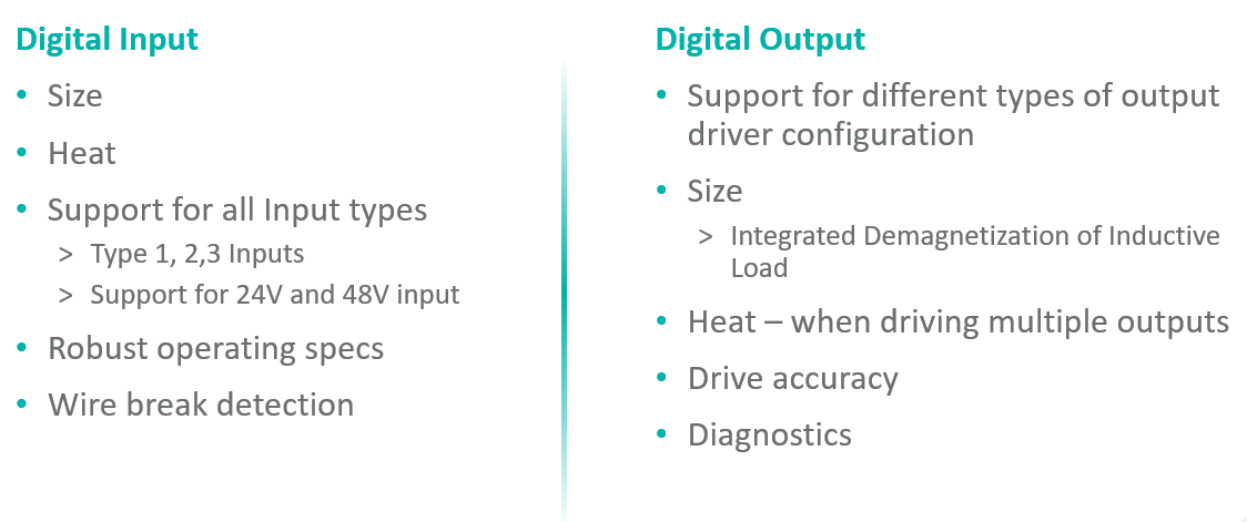 Figure 1. Considerations for Digital Input and Output Modules
For digital inputs, note that it supports various input types, including Class 1/2/3 inputs, and in some cases, 24V and 48V inputs. In all scenarios, reliable operating characteristics are paramount, and even open-circuit detection is critical.
For digital outputs, the system employs different FET configurations to drive loads. The precision of the drive current is typically a key consideration. Diagnostics must also be factored in for many applications.
Below, we explore how integrated solutions can help address some of these challenges.
Designing High-Channel-Density Digital Input Modules
Traditional discrete designs employ resistor divider networks to convert 24V/48V signals into signals usable by microcontrollers. Discrete RC filters may also be used in the front end. External optocouplers are sometimes employed when isolation is required.
Figure 2 illustrates a typical discrete approach for constructing digital input circuits.
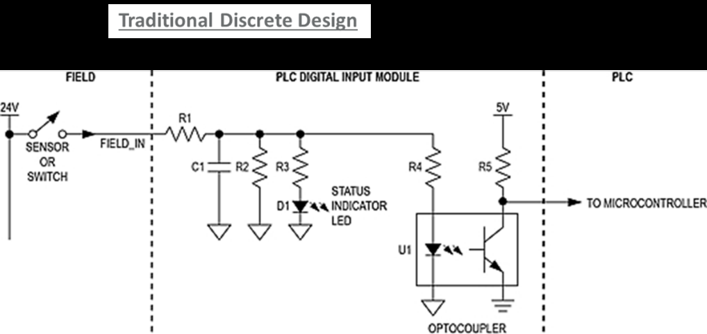 Figure 2. Traditional Digital Input Design Using Discrete Logic
This type of design is suitable for a certain number of digital inputs, specifically 4 to 8 per board. Beyond this number, the design quickly becomes impractical. This discrete approach introduces various issues, including:
● High power consumption and associated hot spots on the board.
● Each channel requires a separate optocoupler.
● Excessive components lead to low FIT rates and may necessitate larger devices.
More critically, the discrete design approach implies that input current increases linearly with input voltage. Consider a 2.2KΩ input resistor and 24V VIN. When the input is 1 (e.g., at 24V), the input current is 11mA, equating to a power dissipation of 264mW. An 8-channel module consumes over 2W, while a 32-channel module exceeds 8W. See Figure 3 below:
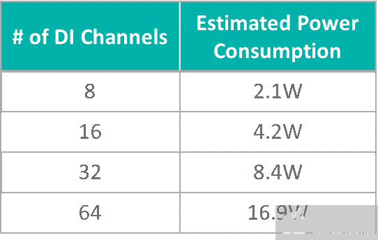 Figure 3. Estimated Power Consumption of the Digital Input Module Constructed Using Discrete Logic
From a thermal perspective alone, this discrete design cannot support multiple channels on a single board.
One of the key advantages of integrated digital input designs is significantly reduced power consumption, thereby minimizing thermal requirements. Most integrated digital input devices allow configurable input current limiting to substantially lower power consumption.
When the current limit is set to 2.6mA, power consumption drops significantly to approximately 60mW per channel. The rated power consumption for an 8-channel digital input module can now be set below 0.5 watts, as shown in Figure 4 below:
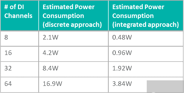 Figure 4. Estimated Power Savings for Digital Input Modules Using Integrated DI Chips
Another reason against using discrete logic designs is that DI modules sometimes must support different input types. The IEC-published standard for 24V digital inputs specifies Types 1, 2, and 3. Types 1 and 3 are typically used together because their current and threshold limits are very similar. Type 2 has a higher current limit of 6mA. With a discrete approach, redesign may be required since most discrete components would need updating.
Integrated digital input products generally support all three types. Essentially, Type 1 and Type 3 are typically supported by integrated digital input devices. However, to meet the minimum 6mA current requirement for Type 2 inputs, two channels must be connected in parallel for a single field input. Only the current-limiting resistor needs adjustment. This requires a minor PCB modification.
For example, current ADI DI devices have a 3.5mA/channel current limit. Therefore, as shown in the figure, when two channels are used in parallel and the system must accommodate Type 2 inputs, the REFDI and RIN resistors must be adjusted. For some newer components, the current value can also be selected via pins or software.
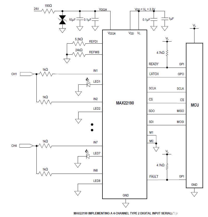
Figure 5. Using two channels in parallel to support two-type digital inputs
To support 48V digital input signals (not a common requirement), a similar process is required, necessitating the addition of an external resistor to adjust the voltage threshold at the field end. Set the value of this external resistor such that the pin's "current limit * R + threshold" meets the voltage threshold specification at the field end (refer to the device data sheet).
Finally, since the digital input module connects to sensors, the design must meet reliable operational characteristics. When using a discrete solution, these protection features must be carefully designed. When selecting an integrated digital input device, ensure the following are determined according to industry standards:
● Wide input voltage range (e.g., up to 40V).
● Capability to use field power (7V to 65V).
● High ESD tolerance (±15kV ESD air gap) and surge capability (typically 1kV).
Providing overvoltage and overtemperature diagnostics is also beneficial to enable the MCU to take appropriate actions.
Designing High-Channel-Density Digital Output Modules
A typical discrete digital output design features an FET with a driver circuit, driven by a microcontroller. Various methods can be used to configure the FET to drive the microcontroller.
An upper-side load switch is defined as one controlled by an external enable signal that connects or disconnects the power supply from a given load. Compared to a lower-side load switch, an upper-side switch supplies current to the load, while a lower-side switch connects or disconnects the load's ground connection, drawing current from the load. Although both use a single FET, the issue with lower-side switches is that the load may short to ground. High-side switches protect the load by preventing ground shorts. However, low-side switches are less expensive to implement. Sometimes, the output driver is also configured as a push-pull switch, requiring two MOSFETs. See Figure 6 below:
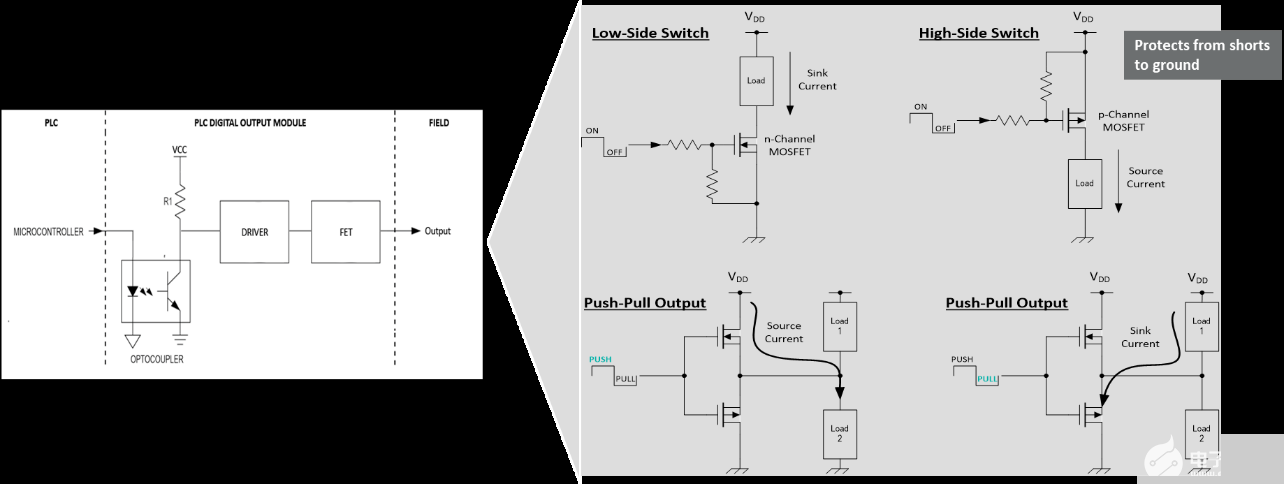 Figure 6. Different configurations used for the digital output driver
Integrated DO devices can combine multiple DO channels into a single component. Since high-side, low-side, and push-pull switches employ different FET configurations, distinct devices can be used to implement each type of output driver.
Built-in Demagnetization for Inductive Loads
A key advantage of integrated digital output devices is their built-in demagnetization capability for inductive loads.
An inductive load is any device containing a coil that, when energized, typically performs mechanical work-such as solenoid valves, motors, and actuators. The magnetic field generated by current can move switch contacts in relays or contactors to operate solenoid valves, or rotate the shaft of a motor. In most cases, engineers use high-side switches to control inductive loads. The challenge lies in discharging the inductor when the switch turns off and current ceases to flow into the load. Negative effects from improper discharge include: relay contacts may arc, large negative voltage spikes can damage sensitive ICs, and high-frequency noise or EMI is generated, ultimately impacting system performance.
In discrete solutions, the most common approach for discharging inductive loads is using a freewheeling diode. In this circuit, when the switch is closed, the diode is reverse-biased and does not conduct. When the switch opens, the negative supply voltage across the inductor forward-biases the diode, dissipating stored energy by conducting current through it until a steady state with zero current is reached.
For many applications, particularly industrial ones where each I/O card has multiple output channels, this diode is often large, significantly increasing cost and design footprint.
Modern digital output devices implement this functionality internally using an active clamping circuit. For example, ADI employs a patented SafeDemag™ feature that enables digital output devices to safely turn off loads without being constrained by inductors. For more details, click here to access the application note on the website.
When selecting digital output devices, several critical factors must be considered. Carefully review the following specifications in the data sheet:
● Check the maximum continuous current rating and ensure multiple outputs can be paralleled when needed to achieve higher current drivers.
● Verify the output device can drive multiple high-current channels (exceeding the temperature range). Consult the data sheet to ensure on-resistance, supply current, and thermal resistance values are as low as possible.
● Output current drive accuracy specifications are also critical.
Diagnostic information is vital for recovering from certain out-of-range operating conditions. First, diagnostic information for each output channel is desirable. This includes temperature, overcurrent, open-circuit, and short-circuit detection. From a chip-level perspective, important diagnostics include thermal shutdown, VDD undervoltage, and SPI diagnostics. Look for some or all of these diagnostics in integrated digital output devices.
Integrating DI and DO on the IC enables the creation of configurable products. This is an example of a 4-channel product that can be configured as either inputs or outputs.
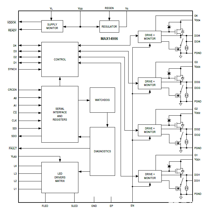 Figure 7.4 Configurable DI/DO Products for Channel Implementation Solutions
It features a DIO core, enabling individual channels to be configured as DI (Type 1/3 or Type 2) or digital output in high-side or push-pull mode. The current limit on DO can be set from 130mA to 1.2A. Built-in demagnetization function. Switching between Type 1/3 and Type 2 digital inputs requires only pin configuration, eliminating the need for external resistors.
These devices are not only easy to configure but also rugged enough for industrial environments. This translates to high ESD protection, power supply voltage protection up to 60V, and line-to-ground surge protection.
This serves as an example of how an integrated approach can unlock greater possibilities (configurable DI/DO modules).
When designing high-density digital input or output modules, discrete solutions become impractical once channel density exceeds a certain threshold. Integrated device options must be carefully evaluated for thermal management, reliability, and size considerations.
When selecting integrated DI or DO devices, key data points warrant attention, including reliable operating characteristics, diagnostics, and support for multiple input-output configurations.